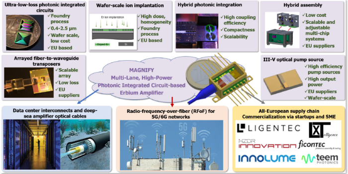
Magnify aims at developing a photonic integrated circuit-based Erbium doped waveguide amplifiers (EDWA) demonstrator (TRL 6), which will be used for early access demonstrator studies with telecommunication companies and enabling iterative feedback.
The invention of the Erbium doped fiber amplifier is arguably one of the most important inventions that has shaped our information society and laid the foundation for optical communications. Rare earth ions provide an ideal gain medium: limiting crosstalk and allowing simultaneous amplification of multiple information carrying channels, while allowing amplification of signals close to the quantum limit. Despite the many advantages of rare-earth ions, their adoption in integrated photonics has been a long-standing challenge. While major effort has been carried out in the 90’ Erbium Waveguide Amplifiers (EDWA), e.g. at Bell Laboratories, these were ultimately abandoned due to the high background loss, large device footprints, and lack of photonic integration manufacturing techniques. Recent advances have heralded the first EDWA based on ion implanted silicon nitride ultra low loss waveguides (Science, 2022).
These devices provide performance already on par with commercial EDFA, with a vastly reduced footprint, wafer-scale manufacturing and ability to create multichannel amplifiers on chip.
Such multi-channel EDWA have applications ranging from data-centers to deep sea fiber amplifiers and general-purpose test and measurement. Within this project, we will move the technology from the laboratory level to TRL6, and commercialize it with partners via a dedicated startup. In addition, as part of this proposal we will develop the require ultra-low loss, implantation ready wafers – the supply chain – and make the available via foundry service via X-Fab in France.
The project therefore addresses technological milestones towards a demonstrator, achieving foundry compatibility, and will engage academic customers for testing in two key areas: optical communications and microwave photonics. By the end of this project EDWA should become a compelling technology proposition and secure strategic investments to build a sustainable business and high tech company.

![Magnify1 Schematic of silicon nitride photonic integrated circuit-based Erbium-doped waveguide amplifier. [EPFL]](https://www.magnify-project.eu/wp-content/uploads/elementor/thumbs/Magnify1-qfqojocsl4rbuaa99dxt8lfjc551gb5weaqdx8ckeu.png)
![EDWA2 Image of an Erbium-doped waveguide amplifier under optical pump. [EPFL]](https://www.magnify-project.eu/wp-content/uploads/2023/11/EDWA2.png)
