
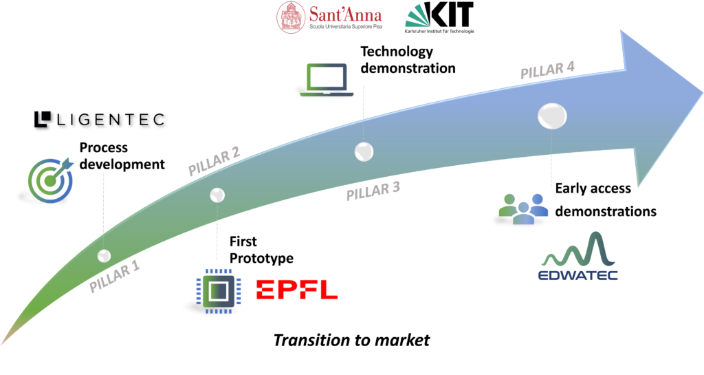
Pillar I: AN200 Si3N4 Process Development for Ion-implantation ready Wafers (LGTF)
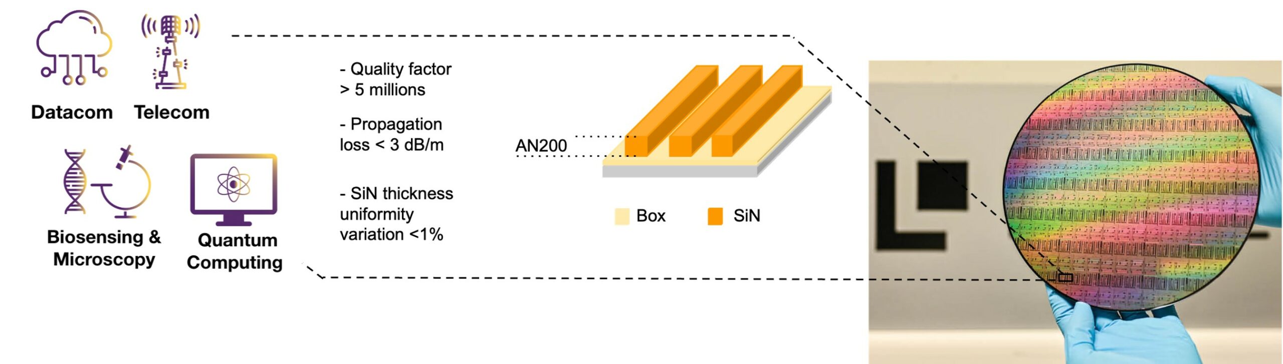
The first pillar of the MAGNIFY projectfocuses on establishing the AN200 Si3N4 process technology in a 200mm CMOS compatible industrial production line by LIGENTEC France. In addition, this initiative aims to deliver world-class performance at an industrial grade while preparing the platform for active integration techniques like ion-implantation.
During the second reporting period, LGTF successfully achieved and surpassed all targeted objectives:
- The AN200 SiN platform development made significant progress toward industrial scale-up, primarily through the successful establishment of the AN200 fabrication line within a CMOS-compatible 200mm production environment.
- Finalized the design and specification of specialized PCM test structures, integrating delay lines, MZI and ring resonators directly onto the wafers. These cells serve as the primary evaluation mechanism for extracting critical performance metrics, such as physical layer dimensions, quality factors, group/effective index and propagation loss.
- LGTF successfully delivered ion-implantation-ready wafers with world-class optical properties, essential for advancing breakthroughs in quantum science, coherent communications, space technologies, and LiDAR.
Key scientific benchmarks achieved include:
- Propagation Losses: Optical losses were lowered to an average of 1 dB/m in the C-band, comfortably exceeding the project milestone of keeping losses strictly below 3 dB/m.
- Quality Factors:Targeted optimization efforts successfully demonstrated an intrinsic Q-factor of up to 6.94 million for both 1.5 µm and 3.0 µm waveguide widths
Pillar II: Prototype Development
The second pillar of MAGNIFYaims to develop a prototype of a fully integrated multiple-lane erbium-doped waveguide amplifier (EDWA), and to ship the device to partners and early access demonstrator clients after comprehensive performance evaluation. This is to be realized by applying high-concentration erbium ion implantation to low loss silicon nitride photonic integrated circuits, which is based on a patented technology by EPFL in 2022. This technology development includes the device simulation, ion implantation recipe optimization, the preparation and submission of the wafer design layout, post wafer-scale processing, and systemic tests. The target devices are expected to simultaneously integrate key on-chip components such as WDM couplers, power splitters, and gain spiral waveguide, which can facilitate the miniaturization of the entire amplifier devices.
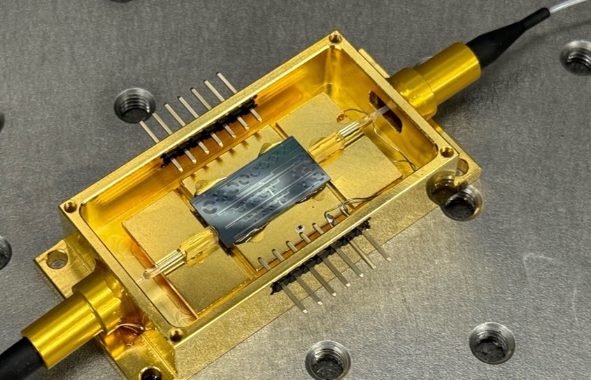
In Year 1, EPFL fabricated 200 nm thick Si3N4 wafers for proof-of-concept demonstration of a new Er-doped integrated photonic platform, optimized erbium doping fluences in the thin-nitride photonic wafers through several commercial vendors, measured passive loss, established a mature WDM coupler library that are consistent with simulations, successfully measured off-chip (fiber-to-fiber) net gain in samples up to 17 dB using a 1480 nm pump. EPFL performed in-house packaging in butterfly modules of selected erbium-doped chips and measured off-chip net gain of 15 dB in a packaged single-lane hybrid integrated EDWA. To investigate the potential of mass-production and the compatibility of the entire manufacturing processes with commercial industrial wafer foundries, EPFL has taped out the photonic circuit designs and submitted it to LIGENTEC France for 8-inch wafer fabrication, which will produce wafers ready for subsequent wafer-scale ion implantation and post processing.
In year 2-3, EPFL updated design to include bundled 8-lane spirals and fabricated Si3N4 wafers, performed an Er doping, measured passive losses and off-chip net gain up to 24 dB in EDWA chips in all 8 lanes independently. EPFL performed successful in-house packaging in butterfly modules of 8-lane hybrid integrated EDWAs using 8-lane fiber array unit (FAU) and measured off-chip net gain exceeding 20 dB for each lane in the packaged device.

Pillar III: Demonstration of Technology
The third pillar of MAGNIFYaims to demonstrate the full potential of our integrated Erbium-Doped Waveguide Amplifier (EDWA) technology—in both single-lane and multi-lane configurations—across two high-impact domains: coherent communications and microwave photonics.
While these advanced applications previously relied on bulky equipment, the completion of the MAGNIFY project marks a major milestone. Through experimental testing and real-world implementation, we have successfully bridged the gap between early lab prototypes and robust, market-ready photonic devices.
Our results prove that whether boosting a single high-power channel or managing multiple parallel data streams, these compact chips can seamlessly handle the speed, power, and bandwidth requirements of next-generation optical networks, 5G/6G systems, and radar communications.
Our amplifier chip strengthens light signals in eight parallel channels at once. That amplifying power is also its weak point: if even a small amount of light is reflected back into the chip, it can start amplifying its own echo instead of the signal we care about. Getting light in and out cleanly is therefore the hardest part of building the device. The team at KIT tackles this with microscopic 3D-printed lenses, printed directly onto the chip and onto the glass fibers that carry the light. The picture above shows the idea demonstrated with a laser [1]. Because every surface these lenses present to the light is tilted or strongly curved, stray reflections are deflected away instead of travelling back into the chip. The same approach is now used to connect our amplifier to its fibers. It also makes assembly far more forgiving — the parts no longer have to be aligned to within a fraction of a hair’s width — and it copes well with high light intensities, giving a robust, reliable package.
With these packaged devices, KIT has put the technology to work in real experiments — sending data at very high speeds through optical fiber, and capturing extremely fast signals for processing [2]. The results show that a single chip, small enough to sit on a fingertip, can handle the fastest and most demanding signals used in optical communications today. Until now, that level of performance required bulky bench-top equipment.

Reference:
[1] Y. Xu et al., “3D-printed facet-attached microlenses for advanced photonic system assembly,” gxjzz, vol. 4, no. 2, pp. 77–93, Nov. 2023, doi: 10.37188/lam.2023.003.
[2] D. Fang et al., “320 GHz photonic-electronic analogue-to-digital converter (ADC) exploiting Kerr soliton microcombs,” Light Sci Appl, vol. 14, no. 1, p. 241, Jul. 2025, doi: 10.1038/s41377-025-01778-1.
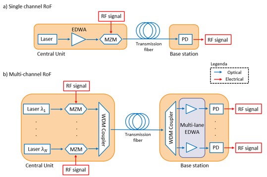
Connecting radar and high-speed communications through optical fibers allows data to travel at the speed of light with virtually no delay. The main hurdle, however, is that optical signals naturally lose strength as they travel down long fiber links, causing the data to get lost in background noise.
To solve this, the teams at EPFL and EDWATEC built a ultra-compact amplifier chip module, which was then put to the test by SSSA in real-world conditions. First, using a single-channel version, the team proved that the chip could dramatically boost weak signals without adding unwanted distortion, even after traveling through kilometers of fiber, severely degraded data was fully restored.
Next, the team scaled up the design into a single chip containing eight parallel amplifier lanes to power complex radar antennas and dense networks. By carefully managing heat and preventing adjacent channels from interfering with each other, all eight channels operated simultaneously with clear transmission.
By replacing heavy, bulky bench-top equipment with a single package intgegrated device, these experiments prove that our technology is ready for real-world deployment in next-generation radar, wireless networks, and high-capacity telecommunications.

Reference:
[1] L. Rinaldi et al., “Photonic integrated technologies for future radio-over-fiber systems”, APL Photonics 1 November 2025; 10 (11): 111101. https://doi.org/10.1063/5.0289727
[2] F. Scotti et al., “Evaluation of an Erbium Doped Waveguide Amplifier RF performance in Microwave Photonics Applications,” 2026 Optical Fiber Communications Conference and Exhibition (OFC), Los Angeles, CA, USA, 2026, pp. 1-3.
Pillar IV: Early access demonstrator studies
The fourth pillar of the MAGNIFYfocuses on early access demonstrator studies to engage industry partners and R&D labs with the cutting-edge Erbium-Doped Waveguide Amplifiers (EDWA) and the AN200 process developed by the consortium. This approach aims to foster collaboration, gather valuable feedback, and drive iterative improvements to ensure the technologies meet real-world demands and pave the way for successful commercialization.
During the first year of the project, significant strides have been made in presenting these technologies at major industry tradeshows and initiating discussions with potential early adopters. Key events included the SPIE Photonics West 2024 and the Optical Fiber Communication (OFC) conference, where the EDWA technology garnered attention for its potential applications in various high-demand sectors such as optical interconnects in data centers, long-haul optical communication, and satellite free-space communications.
Achievements in year 1 of the project:
- Trade Show Participation:EDWATEC actively participated in several major tradeshows, including Photonics West 2024 and OFC 2024, showcasing the EDWA technology to a broad audience. These events facilitated numerous discussions with potential customers, providing insights into market needs and application requirements.
- Feedback and Iteration:The interactions at these events underscored the high interest in compact, power-efficient optical amplifiers for data center interconnects, long-haul communication, and satellite communications. Feedback will be utilized to refine the EDWA designs, focusing on polarization handling, power consumption, and output power requirements.
- Collaborations:EDWATEC established preliminary communication channels with several companies in the optical communication sector, laying the groundwork for future collaboration and evaluation of the early access demonstrator devices.
During Years 2 and 3, EDWATEC engaged prospective customers through major international trade shows and direct technical consultations, supplied packaged and unpackaged EDWA devices to four customers, and consolidated product requirements for in-line, booster, and turnkey amplifier configurations. Customer feedback confirmed that the demonstrated gain, output power, saturation power, and noise figure satisfy the principal performance requirements for the targeted applications. For coherent-transceiver markets, however, a 980 nm pump architecture is considered essential, while wall-plug and optical conversion efficiencies must remain competitive with established EDFAs. Customers also highlighted the need to standardize the Si₃N₄ waveguide thickness for compatibility with existing silicon-photonics and SiN foundry processes, and extend operation into the L-band. For practical evaluation, customers strongly preferred a fully integrated single-box demonstrator incorporating pump lasers and control electronics.
LGTF complemented these activities by assessing the market adoption and application potential of the AN200 platform, including its scalability to 200 mm foundry production and its relevance to data-center interconnects, optical sensing, LiDAR, quantum photonics, and precision metrology. The consolidated commercial and technical feedback was transferred to the project partners.